The purpose of this manual is to describe the functionality and contents of the
easyFPGA-Spartan-6 development board from
LogiFind.com. This document includes instructions for operating the board, descriptions of the hardware features, and explanations of the test code programmed into the on-board programmable memory. For reference design documentation and example projects, see the official website:
www.LogiFind.com
The
easyFPGA-Spartan-6 development board provides a complete hardware environment for designers to accelerate their time to market.The kit delivers a stable platform to develop and test designs targeted to the low-cost and low-power Xilinx Spartan-6 FPGA. The installed Spartan-6 FPGA LX9 device offers a prototyping environment to effectively demonstrate the enhanced benefits of low-cost Xilinx FPGA solutions. Reference designs are included with the kit to exercise standard peripherals on the evaluation board for a quick start to device familiarization.
The
easyFPGA-Spartan-6 development board contains the following individual pieces:
●The easyFPGA-Spartan-6 development board
●USB 2.0 cable
●Xilinx ISE® Design Suite (IDS) 14.7
●Example Source Code
●easyFPGA-Spartan-6 Development Board Users Manual
Please note that this kit does
NOT include a Xilinx programming cable.
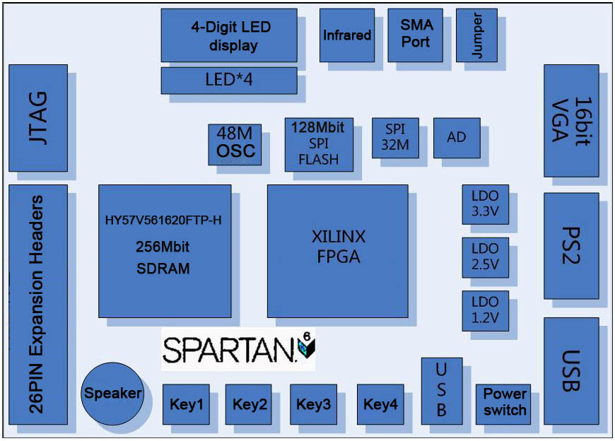
Figure 1. Block Diagram
Figure 1 gives the block diagram of the
easyFPGA-Spartan-6 development board. To provide maximum flexibility for the user, all connections are made through the Xilinx Spartan-6 FPGA device. Thus, the user can configure the FPGA to implement any system design.
Following is more detailed information about the blocks in
Figure 1:
FPGA
Xilinx Spartan-6 XC6SLX9 FPGA
JTAG Port
On-board JTAG Port for programming
SDRAM
One
HY57V561620FTP-H 256M Single Data Rate Synchronous Dynamic RAM memory chip
Flash memory
One
W25Q128 128M NOR Flash memory
One
W25Q32 32M SERIAL FLASH MEMORY for firmware
PS2 Port
Provides the PS2 port for Mouse and Keyboard
Pushbutton switches
4 User Keys
Normally high; generates one active-low pulse when the switch is pressed
Infrared Receiver
Communicate with a Remoter for wireless control
General User Interfaces
4 User LEDs (Active low)
4 digit 7-segment displays (Active high)
Active Type Buzzer
System Clock inputs
48MHz oscillator
VGA output
Uses a 8-bit resistor-network DAC under RGB565 Mode
With 15-pin high-density D-sub connector
AD Circuit and SMA input
Use an AD chip
Use a SMA port for AD signal input
Voltage Regulator Circuit
Provides 1.2V,2.5V and 3.3V for system power supply
Jumper
Selection for External or on-board AD signal source.
On-board USB to TTL/RS232 Module
Use PL2303 for USB-TTL/RS232 Converting (Without DB-9 serial connector)
26-PIN Expansion Headers
Spartan-6 I/O pins, as well as 3 power and ground lines, are brought out to the 26-pin expansion connectors
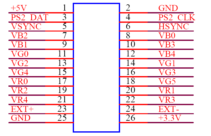 Figure 2.
 26-PIN Expansion Headers
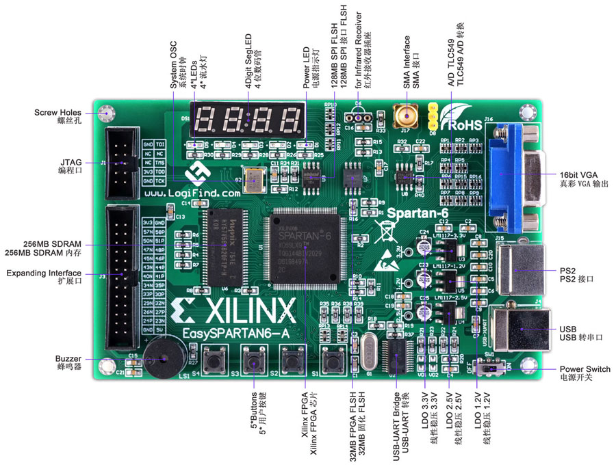 Figure 3.
 What’s on Board
A photograph of the
easyFPGA-Spartan-6 development board is shown in following
Figure 3. It depicts the layout of the board and indicates the location of the connectors and key components.
The following hardware is provided on the
easyFPGA-Spartan-6 development board:
Xilinx XC6SLX9 FPGA Device
JTAG Port for JTAG Programming
256Mbite SDRAM
128Mbite Flash Memory
32Mbite Flash Memory
SP2 Mouse/Keyboard Connector
Four User Keys
26-pin Expansion Headers
Four User LEDs
48MHz oscillator for clock sources
VGA connector
USB to RS232 transceiver
Speaker
1.2V/2.5V/3.3V Voltage Regulator
SMA Port for ADC Input source
ADC
Infrared Receiver
4-Digit LED Display
1) Schematic
2) PCB
3) Datasheet
4) User Manual
5) IO configuration
6) Examples